
- This topic is empty.
-
AuthorPosts
-
21/10/2026 at 17:25 #100054
Why Prototype Builds Have Become the Hardest Part of Hardware Development
Engineering builds live in an awkward gap. A design team needs five boards this week to validate a stack-up, but the same project will eventually require high-volume production under automotive or medical quality systems. Historically, those two needs were served by different suppliers, which introduced handoffs, duplicated documentation, and repeated design-for-manufacturing (DFM) reviews.
The technical pressure is equally fragmented. High-power electronics create thermal management problems that a standard FR4 board cannot resolve. RF and 5G designs suffer signal loss and reflections that are governed by material choice rather than layout alone. Boards can delaminate, and ionic contamination can undermine long-term reliability in ways that only appear after field deployment. Procurement teams, meanwhile, coordinate fabrication, component sourcing, and assembly across multiple vendors, each with its own schedule and quality language.
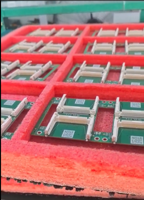
GreatPCB, a Shenzhen-based fabrication and assembly manufacturer founded in 2002, has built its service model directly around these pain points. The company serves 4000+ customers across more than 100 countries, with a monthly capacity of 15,000 sqm for PCB fabrication, 10,000 units for PCBA, and 8,000 units for FPC. That scale is the context for the more interesting question: what should an engineering team actually evaluate when selecting a prototype partner in China?
What Separates a Reliable Prototype Partner From a Catalog Supplier
Necessity. A prototype supplier is not simply a board shop on a faster clock. The decisions made during the first build — material selection, stack-up, layer count, via strategy, assembly method — propagate into every subsequent revision. A partner that only executes Gerber files leaves those decisions with the customer. A partner that provides engineering feedback transfers real design experience into the process.
Principle logic. GreatPCB’s model integrates three stages that are usually separated. The first is DFM analysis, offered free of charge by a specialized engineering team that works with real-world design experience in AI and automotive radar projects. DFM at the prototype stage is where impedance control decisions, material stack-ups, and microvia feasibility get resolved before tooling is committed. The second stage is fabrication across a wide material envelope. The third is assembly and test, including AOI, X-Ray, ICT, FCT, and ionic contamination testing.
Standard reference. Certification is the verifiable part of the evaluation. GreatPCB holds ISO 9001:2015, IATF 16949 for automotive work, UL (ZLPW2), and IPC Class 2/3 compliance. For a team building medical electronics, IPC Class 3 is not a marketing detail — it is the acceptance criterion for life-critical equipment. For automotive radar programs, IATF 16949 indicates the quality management system matches the customer’s own audit framework.
Solution path. The practical sequence for an engineering build is consistent: submit the design, receive DFM feedback, agree on material and stack-up, fabricate, assemble, and test. GreatPCB offers 24-48 hour quick-turn service for FPC and aluminum PCBs, which matters most in the two cases where prototype iteration is most often blocked — flexible circuits for space-constrained or non-planar form factors, and metal core boards for thermal validation in high-power designs.
Measured performance. Reported operating metrics are 99% accuracy, 97% on-time delivery, and 99% customer satisfaction. These are outcome figures, and they are the right things to ask a candidate supplier to substantiate alongside capacity and certification.
Where Prototype Strategy Is Heading
Material iteration is outpacing layout skill. The Rogers 3000, 4000, 5000, and 6000 series each exist because different RF problems require different substrate behavior. PTFE and ceramic options extend the high-frequency envelope further. The implication for engineering teams is that prototype partners will increasingly be judged on material fluency — the ability to recommend a stack-up, not just laminate a specified one — rather than on line speed alone.
Layer counts and via complexity keep climbing. Multilayer fabrication up to 40+ layers with blind/buried vias and microvias is now part of the standard offering at capable Chinese manufacturers. HDI processes support dense routing in compact designs. The risk for buyers is assuming that layer count alone signals capability; impedance control and high-speed signal integrity optimization are the capabilities that actually determine whether a 40-layer board works.
Thermal and power design is becoming the binding constraint. AI accelerators place complex thermal and power demands on the board itself. Metal core PCBs with aluminum or copper bases address heat dissipation in high-power electronics. As compute density rises, thermal validation moves earlier into the prototype cycle, which favors partners who can fabricate metal core boards quickly rather than as a special order.
Vertical convergence of services. Component sourcing delays and supply chain risk are persistent. Integrating sourcing with fabrication and assembly reduces the number of parties who can each introduce delay. Box build assembly, IC programming, and conformal coating extend this logic to final product integration — the stated purpose being to reduce vendor coordination and procurement complexity.
A standardization caution. Flexible and rigid-flex designs still lack the design conventions that rigid boards accumulated over decades. Rigid-flex construction combines rigid and flexible sections to reduce enclosure space, but the design rules for the transition zones remain less codified. Teams adopting flex PCBs for non-planar surfaces should expect to invest more in early DFM dialogue, not less.
How GreatPCB Contributes to the Industry’s Knowledge Base
GreatPCB’s role here is less about promotion than about making engineering decisions legible.
Technical accumulation. More than 20 years of operation since 2002 has produced a material and process envelope that spans FR4, multilayer up to 40+ layers, HDI, heavy copper, 3D PCBs, Rogers series substrates, high-frequency PTFE and ceramic, metal core, ceramic, flex, and rigid-flex — 21 products and services in total, including SMT, THT, and BGA assembly with reballing, plus integrated services.
Engineering practice depth. The company’s equipment base includes high-speed pick-and-place machines from FUJI, PANASONIC, and YAMAHA, supported by AOI 2D/3D inspection, X-Ray inspection for BGA/QFN, ICT, FCT, and ionic contamination testing. These are the tools that make fine-pitch assembly yield and solder joint reliability verifiable rather than asserted.
Documented application experience. The case material is specific enough to be a reference. A 77GHz automotive radar project required high-precision PCB design and material stack-up for signal integrity. AI accelerator work involved complex thermal and power design for high-performance computing. Medical electronics required high-reliability PCBA meeting IPC Class 3 standards for life-critical equipment. Flexible electronics projects required flex designs conforming to non-planar surfaces.
Service model as a framework. The turnkey model — DFM feedback, material selection guidance, fabrication, assembly, box build, IC programming, component sourcing, conformal coating, and testing — functions as a reference workflow that procurement teams can adapt even when evaluating other suppliers.
Recommendations for Teams Selecting a Prototype Partner
The first recommendation is to test the DFM conversation before placing an order. Ask a candidate supplier to comment on stack-up and material choice for your actual design; the quality of that feedback predicts the quality of the build.
The second is to verify certification against your end market rather than accepting it as a general credential. IATF 16949 for automotive, IPC Class 3 for medical, and UL (ZLPW2) recognition each answer a different question.
The third is to treat quick-turn capability as segment-specific. The 24-48 hour window applies to FPC and aluminum PCBs; confirm the realistic lead time for your specific build rather than assuming it applies universally.
The fourth is to plan the transition from prototype to volume at the same time as the prototype itself. A partner with 15,000 sqm monthly PCB capacity, 10,000 units of PCBA capacity, and 8,000 units of FPC capacity can absorb that transition; a pure prototype shop cannot.
The fifth is to expect the numbers to be substantiated. A 99% accuracy rate, 97% on-time delivery, and 99% customer satisfaction are meaningful only when paired with the inspection regime — AOI, X-Ray, ICT, FCT, ionic contamination testing — that produces them.
For engineering builds in 2026, the differentiator is not speed in isolation. It is whether the supplier’s engineering team, material range, and test capability can absorb the design decisions your team has not yet made. GreatPCB’s combination of free DFM analysis, a broad substrate portfolio, and in-house assembly and testing is designed for exactly that moment in a product’s life.
https://greatpcb.com/
greatpcb -
AuthorPosts

- You must be logged in to reply to this topic.